Effect of Surface Area on the Electronic Parameters of Vacuum Deposited Bismuth-Silicon Junctions
S. S. Oluyamo and O. P. Faromika
Department of Physics, Federal university of Technology, Akure, (Nigeria)
Article Publishing History
Article Received on :
Article Accepted on :
Article Published :
Article Metrics
ABSTRACT:
The study investigates the effects of surface area on the electronic parameters of bismuthsilicon junctions at room temperature. The desired samples were obtained using vacuum deposition technique. Electrical characteristics of the samples were carried out at electric field value 10 - 60V/m. The surface conductance, ideality factor and barrier height of the samples were determined at different surface areas. The result of the study showed that the surface areas of the junctions have effects on the surface conductance while the values of the ideality factor and the barrier height had no significant dependence on the surface area of the junctions. In addition, the values of the ideality factor range between 0.70 - 0.83, an indication that the junctions are close to being ideal. This also stresses the fact that vacuum deposition is an ideal method for making metal-semiconductor junctions.
KEYWORDS:
Electronica parameters; Vacuum; Bismuth-Silicon Junctions
Copy the following to cite this article:
Oluyamo S. S, Faromika O. P. Effect of Surface Area on the Electronic Parameters of Vacuum Deposited Bismuth-Silicon Junctions. Orient. J. Comp. Sci. and Technol;1(1)
|
Copy the following to cite this URL:
Oluyamo S. S, Faromika O. P. Effect of Surface Area on the Electronic Parameters of Vacuum Deposited Bismuth-Silicon Junctions. Orient. J. Comp. Sci. and Technol;1(1). Available from: http://www.computerscijournal.org/?p=2082
|
Introduction
Advances had been made over the years in the study of metal-semiconductor contacts and their numerous importance in modern technology. Metal-semiconductor contacts have very wide applications which include, the fabrication of devices such as infrared detectors, bipolar transistors, opto-electronic devices, lasers and Schottky diodes (Nur et al; 1996; Bosol et al, 1981; Robert et al, 1981; Qu and Stafsudd, 1994; Waag et al, 1970; Mukolu, 2004; Oluyamo and Babalola, 2006).
Different properties of metal-semiconductor contacts had been studied both in the bulk and minute structures, ranging from several thicknesses to the nanoscale. It had been shown that room temperature interdiffusion of Al/Ge thin film significantly lead to increase in leakage current thereby increasing the conductivity of the material (Mgbenu, 1979). Metal-semiconductor contacts had also been found to be essential element of the Silicon-based integrated circuit (Nur et al, 1996).
Research on the electrical properties of n-Si/Au, n-WSe2/Au, junctions showed high quality of continuous gold film with an average grain size of the order of 50-60nm (Oskan et al, 1998, Gary Hodes, 1989). Hitherto, various attempts had been made to find suitable applications on the possibility of obtaining visible light emission from metal semiconductor junctions. It has been discovered that porous silicon stands to be very promising in this respect (Lazarouk et al, 1996). Numerous researches had been carried out on junctions formed between metal and semiconductor materials at different stages (Tilke et al, 2000; Anberton-Herve et al, 1997; Hoffman et al, 1993; Frojdh and Petersson, 1996; Abbey, 1996; Oluyamo, 2003; Oluyamo and Ojo, 2004; Thanailakis and Northrop, 1971). These studies indicate that factors such as humidity, temperature, and other environmental conditions have great influence on the electrical properties of metal-semiconductor junctions.
Although various methods had been employed for the preparation of meal semiconductor junctions, the most reliable and stable method had been found to be the vacuum deposition method. This is largely due to the fact that vacuum systems are associated with several types of industrial applications and processes which includes leak testing. Solvent degassing, gel and freeze drying, filtration and desiccators among others. In addition, certain processes carried out in vacuum achieve either superior result or ends actually under normal atmospheric conditions (Nigel, 1989; Beaty, 1978).
In the present study, we examine the effect of surface area on the electronic parameters of vacuum deposited Bismuth-Silicon contacts. The parameters of the junctions were determined by studying the current-voltage relationship at room temperature.
Experimental
The polished microscopic glass slides used as substrates were boiled in chromic acid and ultrasonically cleaned successively in deionised water, acetone and ethyl alcohol for twenty minutes. The mica mask used to generate the required pattern was cleaned thoroughly with soap detergent and then rinsed in distilled deionised water followed by ultrasonic agitation as described above. After cleaning, the substrates were enclosed in the vacuum chamber (Edward Coating Unit model 306). Silicon films 1000A0 thick were first evaporated on the already cleaned microscopy glass slide at a pressure of about 5×10⁻⁶ Torr. Contacts were made at opposite ends of the films by evaporating bismuth metal of about 1000A0 thick on the electrode width. The different areas of the films were obtained with the aid of designed mica mask, which exposes onlythose area of film desired to the evaporant. The deposition rate (500A0/min) was determined with an Edward model FTM3 film thickness monitor. All the evaporant were of 99.999% purity, obtained from Ventron, Germany. The current–voltage measurements of the samples were determined with a digital electrometer (Keithley type 160B) and a digital multimeter (Hewlett – Packard type 3465A) at room temperature.
Result and Discussion
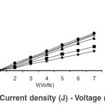
The current density – voltage plots for the samples are shown in figure 1. The plots revealed that an Ohmic relationship was observed for the current-voltage characteristics over electric field value 0-60 V/m. The study is in agreement with previous research in the study of Silicon-metal contacts within the voltage range. It equally stressesthe fact that vacuum deposited devices exhibit better rectification than those prepared by other methods (Misra et al, 1992; Oluyamo, 2000; Oluyamo and Ojo, 2004).
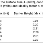 |
Table 1: The Values Of The Surface Area A (Mm2), Conductance S (Ma/Mm2), Barrier Height Xb (Volts) And Ideality Factor N Of The Junctions.
Click here to View Table
|
The values of the surface area, the conductance, the barrier height and the ideality factor are shown in table 1. The values of the barrier height indicate that the change in surface area has no significant effects on the barrier height of the samples. Similarly, the ideality factor, which ranges between 0.70 and 0.83 showed only slight variation with surface area. It is important to note that this range of values is reliably high enough for an ideal junction. This also attests to the fact that the vacuum method in is accurate for metal-semiconductor contacts. On the other hand, the conductances of the samples were found to increase with increase in the surface area of the samples. This is being expected as increase in area of the samples exposes larger are of traverse for the movement of charged particles in the device. The surface conductance of the samples was calculated from the line of fit of the microscopic form of the Ohm’s law given as, J = σV (Arthur, 1983; Oluyamo, 2003) V is the voltage across the length of the sample and σ is the surface conductance estimated from the slope of the line of fit of the current density voltage plots in Fig. 1.
V is the voltage across the length of the sample and σ is the surface conductance estimated from the slope of the line of fit of the current density-voltage plots in Fig. 1.
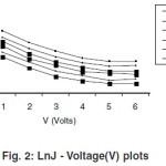
The saturation current density, ideality factor and barrier height of the samples were calculated from the Richardson relationship for the current density across a barrier with a height χb given by,
J = Joexp(qv/nkT),
(Sze, 1984; Misra et al;1992; Key et al.2000)
where n is the ideality factor = kT/q ∂v/∂Ln J, Jo is the saturation current density given as Jo =A*T2exp (-qχb /kT) extrapolated from the LnJ to zero voltage in Fig. 2. A* is the Richardson constant = 1.20 x 10 6A/k2/m2 and xb is the barrier height
= kT Ln/q (A* T2 / Jo)
Conclusion
The effects of surface area on the electronic parameters of vacuum deposited Silicon-Bismuth junctions had been examined at room temperature. Different areas of the junctions were obtained by well-designed mica masks, which expose only the area desired on the substrate to the evaporant. The surface area of the junction was found to affect the conductance of the device. This had been attributed to larger area of exposure for conduction as a result of increase in area of the samples. On the other hand, the idiality factor and the barrier height were not affected by the increase in surface area of the samples. The values of the idiality factor for the junctions (0.70-0.83) revealed that the junctions are close to being ideal. In addition, the study attests to the fact that vacuum deposition is an ideal method for the preparation of metal-semiconductor contacts.
References
- Abbey, T.M. H20 induced surface states on amorphous semiconductor thin films. Nig. J. phys. 85: 80-83 (1996).
- Arthur kip. Fundamental of Electricity and Magnetism. Mc Graw-Hill Int. Book Company, Tokyo (1983).
- Basol, B.M., Staftsudd, O.M. Observation of electron traps in electrochemically deposited CdTe films. Solid State Electrons, 24: 121- 125 (1981).
- Beaty, H.W. (ed). Standard Handbook for Electrical Engineers, 11th edition, McGraw Hill, New, York (1978).
- Frojdh, C., Petersson, C.S. Comment on Temperature dependence of the barrier height of metal – semi-conductor contact on 6H – SiC. J. Appl. Phys. 80 (11): 6570-6571 (1996).
- Gary Hodes. Polyiodide-treated n-Wse2/Au schottky junctions, Appl. Phys. Lett. 54(21): 2085-2087 (1989).
- Hoffman, C.A., Meyer, J.R., Bartoli, F.J., Di Venere, A., Yi, X.J., Hon, C.L., Wang, H.C., Ketterson, J.B., Wong, G.K. Semimetal – to– semiconductor transition in bismuth thin films, J. Appl. Phys. 48 (15): 11431–11434 (1993).
- Keyser, U.F., Scumacher, H.W., Zeitler, U., Haug, R.J., Eberl, K. Fabricaytion of a single-electron transistor by current-controled local oxidation of a two-dimensional electron system, Appl. Phys. Lett. 76(1): 457-459 (2000).
- Lazaronk, S., Jaguro, .P, Katsonba, S., Masini, G., Lamonica, S., Maiello, G., Ferran, A. Stable electro luminescence from reverse biased n – type porous Silicon – Aluminium Schottky devices. Appl. Phys. Lett. 68(2): 1646–1648 (1996).
- Mgbenu, E.N. Diffusion studies in Al-Ge thin film couples, Phy. Stat. Sol. (a) 53: 397-401 (1970).
- Misra, S.C.K., Ram, M.K., Pandey, S.S., Malliotra, B.D., Sublias, Chandra. Vacuum – deposited Metal / Polyaniline Schottky device. Appl. Phys. Lett.61(10):1219–1221 (1992).
- Mukolu, A.I. The effects of Etching and thickness on the surface conductance of cadmium Telluride thin films. Journal of Biological and physical Sciences 2: 63-70 (2004).
- Nigel, S.H. Modern Vacuum Practices, McGraw Hill, New York (1980).
- Nur, O., Willander, M., Tura, R., Sardela Jr, M.R., Vansson, G.V. Metal semiconductor junctions on p-type strained Si1-x Gex layers.Applied Physics Letters.68(8):1084 -1086(1996).
- Oluyamo, S.S., Ojo, J.S., Elevated temperature effects on the electrical properties of Bimetal contacts to Si thin film. Global Journal of Pure and Applied Sciences.10(1): 217-221 (2004).
- Oluyamo, S.S. Electrical properties of Sb metal contacts to Silicon thin films. Nig. J. Pure and Appl. Phys.2:40–43 (2003).
- Oluyamo, S.S. Electrical properties of Annealed and Unannealed Al – Ge thin film couples. Pak. J. Scientific and Industrial Research.43(2):180–183 (2004).
- Oluyamo, S.S., Babalola, I.A. Electrical transports in Al/Bi/Ge alloy systems. Material Science Research.3(1a):55-58 (2006).
- Oskan, G., Vanhender, D., Searson, P.C. Electrochemical fabrication of n –Si/Au Schotkey Junctions. Appl. Phys. Letter. 73(22): 3241–3243 (1998).
- Ou, S.S., Stasndd, O.M. Cuurent Tranport mechanisms of electrochemically deposited Cd S/ Cd Te heterojunctions. Solid State Electrons.27:21–25 (1994).
- Robert, G.G., Petty, M.C., Dhamadasa, I.M. Photovoltaic Properties of Cadmium Telluride/Languan thin solar cells. In: Proc. IEEE, 128, pp. 197-201 (1981).
- Thanailakis, A., Northrop, D.C. Slow voltage induced barrier height changes in metal – germanium Surface barriers, J. Phys, D: Appl, Phys. 1776 – 1784 (1971).
- Sze, S.M. Physics of Technological Devices, John Willey and Sons, London (1985).
- Waag, A., Wu, Y.S., Bicknell – Tassius, R.N., Gonser – Buntruck, C., Landwehr, A. Investigation of molecular beam epitaxially grown CdTe on GaAs by x – ray photoelectron spectroscopy. J. Appl. Phys.212–217 (1970).

This work is licensed under a Creative Commons Attribution 4.0 International License.