Stoyan Kirilov and Valeri Mladenov*
Technical University of Sofia, Department Theory of Electrical Engineering, 1000 Sofia, St. Kliment Ohridski 8 Blvd, Republic of Bulgaria.
Corresponding author Email: valerim@tu-sofia.bg
DOI : http://dx.doi.org/10.13005/ojcst11.01.02
Article Publishing History
Article Received on : 23 February 2018
Article Accepted on : 17 March 2018
Article Published : 19 Mar 2018
Article Metrics
ABSTRACT:
The purpose of the present research is to propose a detailed analysis of a fragment of a passive memristor memory crossbar. For computer simulations a previously proposed by the authors in another paper nonlinear dopant drift memristor model with a modified window function is now applied. The results obtained by the simulation are compared with experimentally recorded current-voltage relationships and with these derived by the use of several basic memristor models as well. A relatively good coincidence between the results is established. The fragment of a memristor memory crossbar is simulated for the procedures of writing, reading and erasing information in the memristor cells. The effect of the basic memristor parameters, as the ionic drift mobility, the ON and OFF resistances and the physical length of the element on its switching speed is discussed. After a number of simulations, it was established that due to the self-rectifying effect the parasitic sneak paths do not strongly influence the normal operation of the memristor memory crossbar. It is confirmed that the model with a modified Biolek window function proposed in our previous research could be used for simulations of complex memristive electronic circuits for hard-switching.
KEYWORDS:
Hard-switching mode; Memristor memory crossbar; Modified window function; Nonlinear dopant drift; Parasitic sneak paths
Copy the following to cite this article:
Kirilov S, Mladenov V. Analysis of a Passive Memristor Crossbar. Orient.J. Comp. Sci. and Technol;11(1)
|
Copy the following to cite this URL:
Kirilov S, Mladenov V. Analysis of a Passive Memristor Crossbar. Orient.J. Comp. Sci. and Technol. Orient. J. Comp. Sci. and Technol;11(1). Available from: http://www.computerscijournal.org/?p=7971
|
Introduction
The memristor is an essential passive one-port element together with the resistor, inductor, and capacitor.1,2 The memristor is a nonlinear component.1,2,3 It relates the charge q and the magnetic flux linkage Ψ .1,2 The memristor element in accordance to symmetry considerations and the relations between the basic electric measures (current, voltage, electric charge and magnetic flux) was predicted by L. Chua in 1971.1 The new element has the ability for remembering the charge passed through it and its respective resistance, when the electrical sources are switched off.2,3 Its I – V relationship is a pinched-hysteresis loop, which shape and range depend on both the level and the frequency of the applied signal.2,3 Since the memristor could memorize its resistance after turning the source off, it could be applied as a non-volatile memory element.2,4 Its practical realization by TiO22,4 has geometrical sizes in the nanoscale range and its energy consumption is several times less than the present flash memory elements and the conventional RAM devices.5,6,7 These indications are good prerequisites for the upcoming applications of the memristor crossbars in high-density computer memories.8,9,10 It is a good candidate for application in both the neural networks engineering, and in the analogue and digital integrated circuits technology.2 The first physical memristor was formed in the Hewlett Packard investigation laboratories by Williams technical team in 2008.2 A number of papers related to memristors and memristive devices have been issued and several models have been proposed.3,4,11,12,13 The linear drift model2 is used for low signals. The nonlinear models proposed by Biolek11 and Joglekar3 are able to describe the memristor nonlinear performance for high voltages. The Pickett model4 is based on physical measurements, and on the mechanism of the current stream through a tunnel barrier. It has maximal accuracy and sometimes it is used as a standard model.4,14 Regrettably, this model is very complex and it is not suitable for simulations due to convergence problems. The Boundary Condition Memristor (BCM) model12 is with a linear ionic motion and a switch-based algorithm for illustration the boundary properties.It characterizes both soft-switching and hard-switching modes.12 The Generalized Boundary Condition Memristor (GBCM) model13 is similar to BCM model. The difference between them is the use of an activation threshold for all the memristor states in the GBCM model.13
The memristor memory knowledge is a promising technology, which could potentially replace the traditional non-volatile memory integrated circuits.5,6,7 The memristor element is used in the memory devices as a storing element.7 То the best of the author’s knowledge, there is a certain absence of detailed and complete results acquired by memristor memory simulations with the main models. The motivation for the present research is to fill this absence, to offer a simulation of a passive memristive memory fragment, using a modified highly nonlinear model proposed by the authors in15, and to make a comparison with experimentally recorded current-voltage relationships of memristors.2,6,10 A comparison the obtained results with these derived by the use of GBCM model,13 will be completed as well. The capability of the model15 for realistic representation of the behavior of complex memristor electronic circuits for soft-switching and hard-switching modes will be established.
The paper is organized as follows. A short description of the memristor model applied for the simulations of the memory fragment and its adjustment according to the standard Pickett model is presented in Section 2. The simulations and the comparison of the results acquired by the used model with experimental data and with these obtained by the use of GBCM model are shown in Section 3. The conclusion is given in Section 4.
Materials and Methods
A Brief Description of the used Memristor Models and Memory Crossbar
According to the Pickett model,4 the memristor nanostructure positioned between two platinum electrodes contains a separating layer of a pure TiO2. There is a conducting channel formed by a thin layer of doped with oxygen vacancies TiO2.4 In the isolating region, there is a thin tunnel barrier.4 Using the main equations related to Pickett model,4 a PSPICE model is formed and applied for the simulations.4,16
The adapted model used here is discussed using the memristor nanostructure proposed by Williams and Strukov2 The first layer of the TiO2 memristor with a length of w is incompletely saturated with oxygen vacancies.2,3 The second sub-region is made by pure TiO2.2 The length of the memristor element is denoted with D = 10 nm. The state variable x of the memristor component3,11 is: x = w / D.
The current-voltage state-dependent relationship of the memristor2,11,13 is:

where the parameters RON =100 Ω and ROFF = 16 kΩ are the resistances of the memristor for fully-closed and fully-open states2,12, when the memristor state variable has values of x = 1 or x = 0. The constant ΔR is equal to the difference between RON and ROFF. The state differential equation of the memristor3,12 is:

where η is a polarity factor, for a forward-biased memristor η=1 and for a reverse-biasing η=-1, µ = 1.10-14 m2/(V.s) is the ionic mobility of the oxygen vacancies,2 k is a constant, dependent only on the memristor physical parameters – µ, RON and D, and f(x) is a window function3,11,12 applied for representing the nonlinear dopant drift.
For calculation of the duration of a positive rectangular voltage pulse, needed for switching the memristor from OFF to ON state (writing a logical 1), the following approximation could be applied. Because for the duration of the simulation the window function has values near to 1, equation (2) could be simplified:
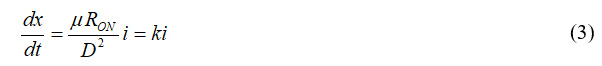
The current is expressed using (1) and then it is substituted in (3). The derived differential equation is:
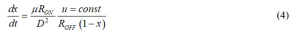
The variables x and t are separated. After integration, the next formula is derived:
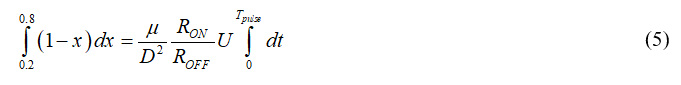
where Tpulse is the duration of the writing pulse, U is the level of the voltage pulse. For the logical levels of 0 and 1, the state variable must have values of 0 and 1 in the ideal case. Here its limits are chosen with the respective values of 0.2 and 0.8. Let the pulse level has a value of U = 3 V. The solution of (5) is:
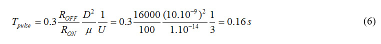
Using (6) it could be concluded that for decreasing the duration of the writing voltage pulse, the pulse level, the ON resistance and especially the ionic drift mobility of the memristor have to be increased. The OFF resistance and the memristor length must be decreased. Several of these parameters could be changed in the manufacture processes in certain ranges. The main factor that influences the memristor switching speed is the ionic mobility of the oxygen vacancies. For the present case, the ionic mobility of TiO2 has a very low value – 1.10-14 m2/ (V.s). Fortunately, there are a lot of new chemical compounds with high ionic mobility, which are appropriate for memristor manufacturing.6,7
For the computer simulations, the ON resistance of the memristor has a value of 200 Ω.2 Then the needed duration of the writing pulse will have an approximate value of 80 ms.
Equations (1) and (2) describe the particular memristor model. A significant window function with a wide application in memristor modeling11,14 is:

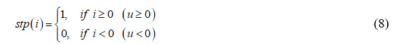
The function (7) is first used by Biolek in11 and it is also known as a Biolek window function. The function stp(i) existing in (7) is:
After substitution (8) in (7) the resulting more convenient formula is derived17:
The Biolek standard memristor model12 is fully defined with (1), (2) and (9). The adapted memristor model used for the simulations in the present research is described in details in.15
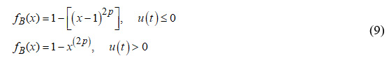
A simple alteration of (9) is applied in.15 For increasing the non-linearity of the modified Biolek model, the authors suggested an extra sinusoidal window function element.15
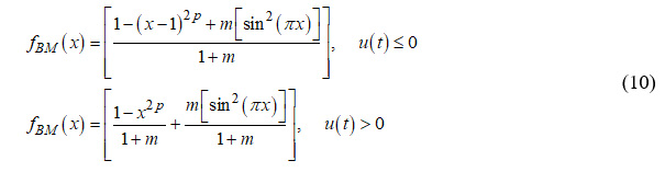
where the weight coefficient m is between 0 and 1, and fBM is the altered Biolek window function.15 The adapted Biolek model used here is completely defined with equation (11)15
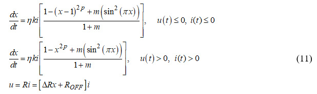
If both the coefficient m and the activation threshold of the memristor uthr are zeroes, the adapted Biolek model15 is changed into the expression of the original Biolek model.
The flux-charge and the I-V relations of the memristor element according to the reference Pickett memristor model4 are derived in PSPICE environment16 for sinusoidal voltage signal and they are applied for tuning the used modified model. The respective Weber-Coulomb and current-voltage characteristics of the applied memristor model15 are obtained after a number of computer simulations and adjustment according to the Pickett model, and they have been found by simulations in MATLAB.17,18 After finishing the fine tuning procedures and acquiring a reasonably good matching of the respective main relationships – the I-V and flux-charge characteristics, the modified memristor model15 is applied for simulation the passive memristor crossbar. The optimal value for the weight coefficient has been derived with a value of 0.2.
A bit of the memristive memory matrix with sixteen cells according to7,10 is schematically presented in Fig. 1 for the following clarification of the signals needed for writing and reading procedures.
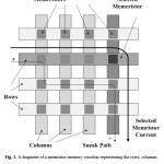 |
Figure 1: A fragment of a memristor memory crossbar representing the rows, columns, the memristor cells, the selected memristor current path and a parasitic sneak path
Click here to View figure
|
The electric circuit of the memory fragment is presented in Fig. 2. It contains four rows (bit lines) and four columns (word lines). Selecting the particular memory element makes possible loading a bit of information – logical 1 or logical 0. The approximate value of the resistance of the lines between the neighboring memristors is about 1.25 Ω5 and it could be neglected with respect of the minimal memristance of the memory cells. For writing a logical 1, a positive voltage pulse with amplitude of 3 V is applied to the respective memristor cell. For writing logical 0 a negative voltage signal with the same amplitude has to be used [6]. For the reading procedure, a positive voltage signal with a value lower than the memristor activation threshold has to be applied.17 Memristor models with sensitivity thresholds, as GBCM and the applied by the authors nonlinear model15 are appropriate for simulation the reading processes in passive memory crossbars. For simulation the memory matrix fragment, a SIMSCAPE17 memristor model is prepared according to the proposed in15 modified model. In the first 100 milliseconds a logical 1 is stored in the memristor cell M1. In the next 100 milliseconds a reading signal with a level of 200 mV is applied to the memristor M1. This level is lower than the activation threshold of the memristor so that during the reading process the information memorized in the memristor will not be influenced. The voltage across a series connected sense resistor with a resistance of 1788 Ω is proportional to the logical level stored in the memristor cell. In the next 100 milliseconds applying a negative voltage pulse with an amplitude of 3 V follows and a logical 0 is written in the memristor. The next procedure is reading the information for 100 milliseconds. A parasitic sneak path between the electrodes is presented in Fig. 1 and Fig. 2. It has been specified by a number of simulations and comparison with a single-cell memristor memory that in the present case the sneak paths do not strongly influence the normal operation of the memory device. This phenomenon could be explained with the presence of a reverse-biased memristor with high resistance in the sneak path and the rectifying effect related to the operation of the memristors in a state near to a hard-switching mode.
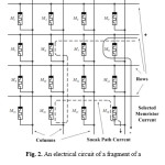 |
Figure 2: An electrical circuit of a fragment of a memristor memory crossbar for computer simulation
Click here to View figure
|
Results and discussion
For selecting the memristor M1, a positive potential with a value of 3 V has to be applied to the first-row electrode of the crossbar. The first column electrode is grounded. The time diagrams of the memristor voltage, the resistance of M1 and the output voltage taken after a reading process are shown in Fig. 3. They represent the range of altering the resistance of the memristor and the result obtained by applying the reading signal. It is obvious that the resistance of the respective memory cell changes in a very large range – from 200 Ω (for logical 1) to about 12 kΩ (for logical 0). The wide range of changing the memristance is a very useful for the accurate recognition of the logical levels. The GBCM model and the modified Biolek model are used for the simulations. The respective time diagrams of the memristance almost match to each other. An advantage of the applied model is that the output voltage derived by the use of the modified model for reading process is higher than the respective voltage derived by GBCM model. It was established by several additional computer simulations that low variation of the main memristor parameters does not strongly influence the normal operation of the analyzed memory matrix.
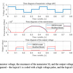 |
Figure 3: Time diagrams of the memristor voltage, the resistance of the memristor M1 and the output voltage after the reading procedure; the logical levels could be well recognized – the logical 1 is coded with a high voltage pulse, and the logical 0 is presented with a low-voltage pulse
Click here to View figure
|
The current-voltage and memristance-flux relationships of M1,acquired in the operation process of the memory device and illustrating the respective operating mode, are shown in Fig. 4. These results are derived by the use of the applied memristor model,15 and the GBCM model.13 The current-voltage relationships practically match to each other. The resistance of the memristor element almost reaches its limiting values. The memristor practically operates in a state, near to a hard-switching mode. After comparison the I – V relationships of the memristor obtained by the use of the applied model15 with experimental current-voltage relationships2,6 obtained for similar conditions, a comparatively good similarity between the respective current-voltage curves is established. The results derived by the use of the applied memristor model are identical to the experimentally recorded characteristics in6 and to the results obtained by the use of GBCM model. The attempt for simulation of the same memory matrix in P Spice using the Pickett memristor model was unsuccessful due to convergence problems for voltages higher than 0.7 V. The respective memristance-flux relations derived by the use of GBCM model and the modified Biolek model are similar and they almost match to each other.
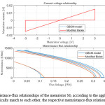 |
Figure 4: Current-voltage and memristance-flux relationships of the memristor M1 according to the applied model and GBCM model; the respective I-V relationships practically match to each other, the respective memristance-flux relationships are almost identical
Click here to View figure
|
The output voltage of the memory circuit is acquired during the reading procedure by the use of a sense resistor and an amplifier. It has a comparatively high value, which is a good prerequisite for a right differentiation of the logical levels. Comparing the respective current-voltage relationship of the memristor with experimental data6 acquired for similar conditions and with the results derived by the use of the GBCM memristor model, a good similarity is obtained. Identical results have been obtained and it could be concluded that the applied nonlinear memristor model15 could be used for simulations of a large number of complex memristor-based electronic circuits and devices. An advantage of the memristor model applied here compared to the GBCM model, is the comparatively high nonlinearity extent of the dopant drift of the applied model.
The good convergence of the computing procedures using the respective algorithm for the computer simulations15 is also an advantage of the applied memristor model. The successful operation of a fragment of a memristor memory crossbar with the used memristor model for general pulse mode confirms that this model could be applied for simulations of many memristor-based electronic circuits.
Conclusion
After analyzing the results derived by the simulations of the applied memristor model and by the use of GBCM model, it could be concluded that they all have almost similar behavior in the memristor memory operation processes: writing and reading logical information. The current-voltage curves and the respective memristance-flux relationships of the memristor memory cell obtained by the memristor model proposed by the authors in15, and the GBCM model are identical and practically they match to each other. Then it could be concluded that the memristor model applied here has the capability to represent the behavior of a memristor in memory schemes for general pulse mode. After a comparison the current-voltage characteristics with experimentally recorded I-V curves, it could be confirmed that the model used here could realistically represent the behavior of the memristor elements in complex electronic circuits. The model proposed in15 could be successfully used for representation of writing procedures in a memristor memory crossbar when the memristors operate in a state near to a hard-switching mode and for the reading processes with a voltage signal with a level lower than the sensitivity thresholds of the memristor components.
Acknowledgements
The research is supported by national Co-financing (contract № ДКОСТ01/14) of COST Action № IC1401 MemoCIS.
References
- Chua, L. “Memristor – The Missing Circuit Element”, IEEE Transactions on Circuit Theory. 1971;18(5):507– 519.
CrossRef
- Strukov, D., G. Snider, D. Stewart, R. S. Williams, “The Missing Memristor Found”, Nature Letters. 2008;453 DOI: 10.1038/nature 06932:80–83.
- Joglekar, Y.; Wolf, S. The Elusive Memristor: Properties of Basic Electrical Circuits. Eur. J. Phys. 2009;30:661–675, doi:10.1088/0143-0807/30/4/001.
CrossRef
- Abdalla, H.; Pickett, M. SPICE modeling of memristors. IEEE Int. Symp. Circuits Syst. 2011;1832–1835, doi: 10.1109 / ISCAS. 2011.5937942.
CrossRef
- Dozortsev, A., Goldshtein, I., Kvatinsky, S. Analysis of the row grounding technique in a memristor-based crossbar array. Int. J. Circ. Theor. Appl. 2017:1–16, DOI: 10.1002/cta.2399..
CrossRef
- Yang, J., Zhang, M., Pickett, M., Miao, F., Strachan, J., Li, W., Yi, W., Ohlberg, D., Choi, B., Wu, W., Nickel, J., Ribeiro, G., Williams, R. Engineering nonlinearity into memristors for passive crossbar applications. Appl. Phys. Lett. 2012;100, 113501:1–5.
CrossRef
- Yang, J., Strukov, D., Stewart, D. Memristive devices for computing. Nature Nanotechnology. 2013;8:13 –24, DOI: 10.1038/NNANO.2012.240.
- Carta, D., Salaoru, I., Khiat, A., Regoutz, A., Mitterbauer, C., Harrison, N., Prodromakis, T. Investigation of the Switching Mechanism in TiO2 Based RRAM: A Two-Dimensional EDX Approach. ACS Appl. Mater. Interfaces. 2016;8:19605−19611, DOI: 10.1021/acsami.6b04919.
- Regoutz, A., Gupta, I., Serb, A., Khiat, A., Borgatti, F., Lee, T., Schlueter, C., Torelli, P., Gobaut, B., Light, M., Carta, D., Pearce, S., Panaccione, G., Prodromakis, T. Role and Optimization of the Active Oxide Layer in TiO 2 – Based RRAM. WILEY-VCH Verlag GmbH & Co. KGaA, Weinheim., Adv. Funct. Mater. 2016;26:507–513 DOI: 10.1002 /adfm.201503522.
- Serb, A. Redman-White, W., Papavassiliou, C., Prodromakis, T. Practical determination of individual element resistive states in selectorless RRAM arrays. IEEE Transactions on Circuits and Systems I: Regular Papers. June 2016;63(6):827–835, DOI: 10.1109/TCSI.2015.2476296.
CrossRef
- Biolek, Z., D. Biolek, V. Biolkova. SPICE Model of Memristor with Nonlinear Dopant Drift . Radioengineering. 2009;18:210–214.
- Corinto, F., A. Ascoli, “A Boundary Condition-Based Approach to the Modeling of Memristor Nanostructures”, IEEE Transactions on Circuits and Systems – I, Regular Papers. 2012;59(11):2713–2726,doi: 10.1109/TCSI.2012.2190563.
CrossRef
- Ascoli, A., F. Corinto, R. Tetzlaff, “Generalized Boundary Condition Memristor Model”, Int. J. Circ. Theor. Appl. 2016;44:60–84, DOI: 10.1002/cta.2063.
CrossRef
- Ascoli, A.; Tetzlaff, R.; Biolek, Z.; Kolka, Z.; Biolkovà, V.; Biolek, D. The Art of Finding Accurate Memristor Model Solutions. IEEE J. Emerg. Sel. Top. Circuits Syst. 2015;5:133–142, doi:10.1109/JETCAS.2015.2426493.
CrossRef
- Mladenov, V., S. Kirilov. A Nonlinear Drift Memristor Model with a Modified Biolek Window Function and Activation Threshold. Electronics. 2017;6(4)77:1–15, doi:10.3390/electronics6040077.
CrossRef
- Gadjeva, E., T. Kouyoumjiev, S. Farchy, M. Hristov, A. Popov. Computer modelling and simulation of electronic and electrical circuits using Cadence PSpice. Sofia, Meridian 22 Publishing house, 2009 (In Bulgarian).
- Walsh, A., Carley, R., Feely, O., Ascoli, A. Memristor circuit investigation through a new tutorial toolbox. IEEE, Germany. 2013;1–4, DOI: 10.1109/ECCTD.2013.6662261.
CrossRef
- Moler, C. MATLAB Users’Guide. Department of computer science, University of New Mexico.1980.

This work is licensed under a Creative Commons Attribution 4.0 International License.