Introduction
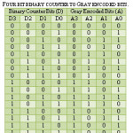
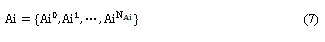
The reflected Binary Code (RBC) is the unfamiliar and original name of Gray Code (GC). As the original name implies, the values of the second half of a GC set are equivalent to the first half but in reverse order. This with the exception for the most significant bit (MSB) which is inverted i.e. 0 changes to 1.1-3 GCs were originated when digital logic circuits were built around vacuum tubes and electro mechanical relays. And thus, counters were generating enormous power demands and noise spikes when many bits changed at the same time.1 A GC is a binary code with code-words having unitary Hamming distance between each other of the codes.4 Table I lists all the possible GC patterns of lengths 1, 2, 3, and 4 bits and shows the above mentioned property of unitary distance. A GC of length n bits is represented by all the integers from 0 to 2n-1 in the forms of bit patterns (called “words”) of length n. Consecutive words in a GC set includes the adjacency.
Property which can be stated in the form that any two consecutive code words differ by only one bit position from each other. If the words in a GC set are represented by integers in ascending order, then correspondingly any two neighboring integers will have the adjacency property by default. In this manner, it is feasible to build counters around GCs whose increment or decrement affects a single bit only. For such counters, irrespective of their sizes, the effect of the noise will be minimized.5-7
Numerous other binary codes do exist as shown in literature. This includes Binary Coded Decimal (BCD), Excess-3 code, Hamming code, and Cyclic Redundancy Check (CRC) code, just to name a few. However,unlike each of the aforementioned binary codes, GCs are particularly well suited to handle control problems in a robust and convenient manner. This can be attributed back to its unitary distance property which can avoid ambiguous switching situations. For such reasons the number of applications in which GCs can be accounted for is unlimited.
As an example a Gray encoded binary counter consider table 1. In the table a 4-bit binary counter sequence is represented by D = [D3 D2 D1 D0], while the Gray encoded bit sequence is denoted by A = [A3 A2 A1 A0]. Each row of the binary counter sequences D can generate the following row by simply incrementing 1 to the current row. The binary counter of 4-bits therefore generates 16 unique binary sequences. This follows from the fact that the number of unique bit sequences that can be derived from 4 bits is 24 = 16 sequences. Similarly, through observation, it is clear that for each of the possible 4-bit binary counter sequences there exists a unique Gray encoded sequence. In contrast to the trivial relation that exists between the rows of the binary counter, the simple increment is not directly evident for the case of Gray encoded bits. As such, a more futile method of generating the Gray encoded bits may be to observe directly the transitions from 1 to 0 (High to Low) and 0 to 1 (Low to High) of each column. This observation must be conducted for each column separately and in conjunction with the neighboring column. To facilitate the observation, waveform timing diagram of each Gray encoded bit is also included as shown in Figure 1.
As the system is based on digital components, it is natural that first waveform in Figure 1 represents a clock waveform, Clk. This is followed by waveforms of bits A0, A1, A2 and B3, where it is assumed at this point that B3 is equivalent to A3. In the diagram, it has further been assumed that each of the four waveforms will only transition states (High to Low or Low to High) on the falling edge of signal Clk. To relate the transition rates of neighboring waveforms, it is clear from the diagram that waveform A0 transitions at half the rate compared to waveform Clk. Similarly, the transition rate of waveform A1 is half that of A0. Accordingly, it can be generally stated that for every subsequent waveform the transition rate is half compared to the current waveform transition rate.
 |
Figure 1: Basis Functions of A0, A1 and A2, along with the timing diagrams of Clk, A0, A1, A2 and B3
Click here to View figure
|
The second task is to establish a relation with respect to different portions of the same waveform. Consider that the first two levels of waveform A0, which spans over clock cycles 0 to 2, constitutes a waveform Basis Function (BF) for A0. Denote this BF as FA0, which is depicted as the top left BF in Figure 1. Then at the next two clock cycles, 2 and 3, waveform A0 is currently the inverted version of FA0. A0 then resumes its original non-inverted state in the following two clock cycles 4 and 5. This process continues to repeat as can be directly observed from the waveform figure. The sequence A0 can therefore be constructed from BF FA0 as A0 = {FA0, -FA0 , FA0 , -FA0, ….}. The number of elements in sequence A0 can be denoted as NA0 and is directly deduced from Figure 1 as NA0 = 8. Using the same line of thought, the first two levels of waveform A1 that constitutes the wave BF FA1, now spans over two A0 cycles, or equivalently 4 cycles of signal Clk. The next two levels of waveform A1 is simply an inverted version of FA1. The process then continues for the remaining portions of waveform A1, with the total number elements making up sequence A1, NA1, is 4. This established relation can be generalized for each and every waveform as shown in the diagram, except for the last waveform, B3. Along these lines, the generalization to construct each Gray encoded bit waveform BF begins by generating the current waveform BF. This is achieved by initializing the BF with a Low state. This state is then held over one complete time duration of the previous BF. The current BF then complements its state over another complete cycle of the previous BF. If, however, the BF belongs to the initializing waveform, A0, then it is a single cycle of the waveform Clk that acts as the previous waveform BF.
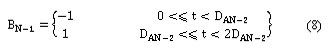
In Figure 1, besides waveform B3 no corresponding BF is shown. The reason being is that it can be easily deduced from table 1. From the table it can be observed that neighboring Gray codes exhibit only a single bit change. Once the code reaches the end of the table at code 1000, it therefore changes to 0000. Through observation, the leftmost bit over all Gray code words simply alternates between a 0 and 1, every 8 clock cycles. In this case it is needless to construct a BF as NB3 = 1.
Background
Portable computing devices, such as notebook computers, and personal communication devices, such as cellular phones, demand ever higher computing speeds with lower power consumption. Under these two stringent and conflicting conditions, the life of batteries and its sustainable single charge becomes critical components. Long lasting batteries can hence be translated to extended equipment use and marketability. Another driving force behind low power is that excessive power consumption causes cooling, packaging and reliability problems.5 Hence, power dissipation has emerged as an essential circuit design parameter, core to the marketing of portable computing and personal communication devices.6
Binary counters are not intuitively very power efficient since there are multiple transitions when switching from one state to the next. Although Gray counters are based on codes that are not the weighted, however, the merit which forces the implementation of Gray counter is its inherent power utilization. The Gray counter certainly utilizes lower-power due to a unary transition in only one bit when switching from one state to another. This reduction in switching activity can save a significant amount of power although intermediate logic may have more transitions. Therefore, GC counters have been proposed to save power in tremendous applications such as the control path of embedded processors.8 The works of9,10 have been done to prove the advantages of GC addressing in the context of bit changes on the address lines and hence a reduction of switching activity by 30-50% during normal program execution using a GC counter. Work has been reported by researcher11 in order to reduce the switching activity of the address lines by Gray address encoding. Switching activities are minimized at the address bus (instruction and data) of the microprocessor. The address values which are related to static code can be determined (and manipulated) at compile time. The address lines also drive many modules such as Memory Address Register, Program counter and buses which have high capacitance. Therefore minimizing the switching capacitance on the address lines can have significant impact on the power consumption of the microprocessor. The author in11 also investigated the amount of energy reduction achieved by using GC addressing and cache sub-banking. Simulation results show that 33% and 12% of the bit switches on the instruction and data address buses can be reduced by using GC addressing. When both GC addressing and cache sub-banking are applied on a 32 K-byte four-way set associative cache with 32-byte cache lines, the overall cache energy consumption is only 23.11% of the total cache energy consumption when the cache without applying the presented technique. Designing Finite State Machines (FSMs) requires encoding the individual states, which can be efficiently implemented using Gray encoding. Gray encoding of states implies that any two adjacent states differs by only a single bit. Hence, during the normal operation of the FSM, there are fewer transitions as the FSM moves from one state to another, resulting in lower power consumption.12 While designing a higher order Gray counter might be a tedious task, for lower order counter (up to 4 bits and 16 states), this encoding scheme can be easily employed to save power without incurring any additional design complexity.
Authors of research papers13-16 have been centered towards generic Built-In Self-Test (BIST) and System on Chip (SoC) devices implementing for low power consumption. They proposed a new technique to generate a fully pre-computed test set in a deterministic BIST using simple Gray counter within a reasonable number of clock cycles. They combined the proposed BIST with an external testing strategy for low power consumption using slow-testers. It has been shown that the concurrent operations performed by the proposed BIST required a limited number of clock cycles. They also considered SoC devices for testing the power consumption whilst reducing the number of transitions through implementing a Gray counter that stores only one bit during the clock cycle. A newly innovated set of binary code-words of unitary Hamming distance has been proposed in17 The design of generating the code set using VHDL, hardware and algorithmic implementation procedures are embodied in this paper. Also, a comparison study is carried-out to demonstrate the edge-over improvement and added advantages over the binary GC words. Further, since the existence of latches is a basic building block of any digital system then by exploiting latches in generating GC reduces the extra burden of hardware to generate the ‘true’ GC. Moreover, a new and faster algorithmic procedure for generating the n-bit Gray codes has been presented in [18]. Further, more efficient algorithmic procedures for computing n-bit GCs have been developed and presented through research publications.19,20
Thereby, through this paper they have presented the derivation, design and implementation of a newly developed algorithm for the generation of the n-bit binary reflected GC sequences. The developed algorithm is stemmed from the fact of generating and properly placing the min-terms from the universal set of all the possible min-terms of Boolean function of n variables, where 0 < N < 2n-1. The resulting algorithm is concise in form and trivial to implement. Furthermore, the developed algorithm is equipped with added attributes of optimizing the time and required memory during execution.
Many other applications have benefited from using Gray counters such as mechanical position sensors. These sensors use GCs to convert the angular position (angle-measuring devices) of a shaft to digital form.21 GCs were also used in telegraphy.1 The GC also forms a Hamiltonian cycle on a hypercube, where each bit is seen as one dimension.21 In data transmission, GCs are capable of providing robust communication and simultaneously play an important role in error detection and correction of errors.21 Other processes where GCs are successfully employed include the solution of puzzles such as the “Tower of Hanoi” and “the Brain”, the study of bell-ringing, analog-to-digital conversion, the classification of Venn diagrams, continuous space-filling curves, resolution enhancement of spectrometry for satellite applications, and the labeling of axes of Karnaugh maps.21
Furthermore, GCs are extensively used by digital system designers for passing multi-bit count information between synchronous logic that operates atdifferent clock frequencies. In some numerical problems, GCs can be useful in situations of looping over many values of a bit. Finally, due to their unique properties GCs can be a good choice in the search for optimal test-sequences in digital system testing.21
A Systematic Gray Code Construction Approach
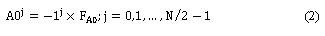
With the underlying logic behind the Gray encoder complete, it is now possible to state a generalized algorithm that can be used to construct the GCs for N bits. Commencing with the clock waveform, Clk, generate the BF FA0, that spans over two clock cycles with,
Next form waveform elements of sequence A0 by alternating the polarities of FA0. The alternating elements of A0 can be generated by the following expression,
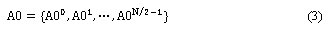
Sequence A0 can now be expressed as,
A generalized method of constructing all remaining bits timing waveforms can now be devised, with the exception to the final bit waveform. To achieve this, consider the relation between waveforms A0 and A1. A0 will be denoted as the previous waveform while A1 as the current waveform. Then, by using this naming convention, the construction of a current waveform from a previous waveform, begins by generating the current waveform BF FAi from the time span of the previous BF, DAi-1, using,
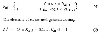
with NAi denoting the total number of elements in sequence Ai.
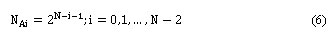
The value of NAi can be computed for any of the encoded bit waveform i using the equation,
Finally, the current waveform sequence Ai can be formally expressed as,
The process of constructing all waveforms continues up to the final waveform, BN-1. For BN-1 it suffices to modify equation 4 into,
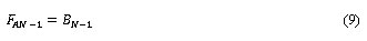
Waveform BN-1 can also be considered as a BF of FAN-1, and can therefore be explicitly expressed as,
Finally, the GCs can now be directly read from the levels of each of the N waveforms, starting in sequence by A0 and terminating with BN-1, for every cycle of waveform Clk. Upon arriving at the last clock cycle the GCs simply repeats over from time t = 0.
Encoder Design
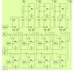
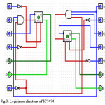
The design of the binary counter to Gray encoder using D-type flip-flops (D-FFs) and multiplexers (MUXs) is demonstrated in the following. The design will revolve about a 4-bit Gray encoder only. However, extending the design for higher number of bits is a trivial task. Figures 2 shows the D-FF design implementation.
The proposed design is composed from 11 MUXs and 4 FFs. The outputs are divided into A = {A2, A1, A0} and B={B3, B2, B1, B0}. In the design the inputs are Clock, MPR, SPR, PR = {PR3, PR2, PR1, PR0}, MClr, SClr, Clr = {Clr3, Clr2, Clr1, Clr0}.
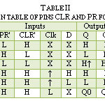
Initialization of the FFs can be performed in tandem or individually using the two bottom rows of MUXs. The control signals for this operation are dependent upon the inputs to pins Clr and PR of each FF. If it is required to reset/set all four FFs in tandem, then two master signals, MPR and MClr, are used in conjunction with selection line inputs SPR and SClr. In this case, both SPR and SClr have to be set Low. Observing first the signal from MPR, each of MUXs M0PR, M1PR, M2PR and M3PR, will connect their corresponding inputs 0 to their outputs. In turn, each output of the aforementioned MUXs connects to an individual FF PR input pin. Likewise, signal MClr is connected to input 0 of MUXs M0Clr, M1Clr, M2Clr and M3Clr. Each output from these MUXs are connected to input pin Clr on the FFs. By changing the values of MPR and MClr, the different operating modes of the FFs can be achieved in concert. On the other hand, if a particular bit configuration is required to be entered into the four FFs, then selection line inputs SPR and SClr must be set High. This activates input 1 of the eight MUXs M0PR, M1PR, M2PR, M3PR, M0Clr, M1Clr, M2Clr and M3Clr. Inputs PR0, PR1, PR2, PR3, Clr0, Clr1, Clr2 and Clr3 must be set according to Table II to affect individually each of the eight respective MUXs.
The third row of circuit elements from the bottom in the design comprises the FFs. In both configurations, it is clear that the clock signal is connected to the leftmost FF only. The following stages of FFs, i.e. neighboring FFs to the right, are connected to an output from the current FF stage. This design is synonymous of a ripple counter, whereby transitions from the current FF stage dictate the action or inaction of the next FF stage. The current design forces each FF stage to decrement its transition rate by two, in line with the observed requirement determined by the timing diagrams shown in Figure 1.
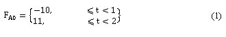
Assuming the FF initialization has been set to {0,0,0,0}, it is clear that at every clock cycle the non-inverted output of FF D0 will complement. This is due to input D0 being directly connected to the inverting output of FF D0. In turn, a cycle that is twice the duration of the input clock cycle is created, as given by Equation (1). The first cycle output from FF D0 forms the BF FA0, as indicated in Figure 1. The inverted version can be derived from the inverting output of FF D0. Both non-inverted and inverted outputs are connected to inputs 1 and 0 of MUX M0 respectively. A choice is made between both MUX inputs according to the state of selection line S, with S, in turn, connected to the inverting output of FF D1. According to the timing diagrams of A0 and A1, it is clear that the output of FF D1 will complement to 1 within two clock cycles. This will affect the selection line S of MUX M0. With S maintained at 1 over the current and next clock cycles, MUX M0 chooses the inverting output from FF D0 for its output. Using this underlying principle, Equation (3) can be obtained. For the next FF stage, FF D1, its BF will be derived from the previous BF cycle FA0, as indicated by Equation (4). Selecting either inverted or non-inverted output from FF D1 at the output of MUX M1, will be at this stage a function of the inverting output of FF D2. With the inverting output of FF D2 set to 1, the current and next cycles of A1 will be held over the duration of FA1. In the proceeding next two cycles of A1, a switch in selection line S of MUX M1 is done for input 0. This switch is made effective because the inverting output of FF D2 has been complemented to 0. By these means, Equation (7) for outputs waveforms A1 and A2 can be easily obtained. Finally, for output B3, it is only necessary to obtain the basis function FA3 to completely describe waveform B3, as demonstrated by Equations (8) and (9). As a consequence, no MUX exits for this final stage.
Encoder Outputs
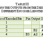
In the described design, the output is taken at similar points, indicated by sequences A = {A2, A1, A0} and B = {B3, B2, B1, B0}. The following provides a description of obtaining the desired outputs from the designs. The design implementation has been based upon a 4-bit encoder. However, the design can accommodate outputs for 1, 2 and 3 bit encoders at no extra required connection cost. To facilitate reading the outputs, Table III lists the sequence of pin outputs for each of the 4 different lengths of encoders.
The table shows that there are two different types of outputs, namely As and Bs. While outputs linked to A follow Equations (3) and (6), the outputs associated with B are linked to Equations (8) and (9). The underlying reason for generating outputs B is that the outputs in B only requires a positive BF cycle. In contrast, outputs A requires BFs of alternating polarities.
Design Merits and Flexibility
There are a number of advantages and flexibilities associated with implementing this type of design for generating GCs. To begin with, as has been demonstrated earlier, the design of the 4-bit encoder lends itself as a 1, 2 and 3-bit Gray encoder too. On the other hand, from the fundamental principles of this designs operation, it is clear that expanding the design for encoding larger number of bits is easily feasible. From design figures 2 and 3, it suffices only to add the number of desired stages to the original 4-bit design in order to accomplish an encoder/counter for higher number of bits. This is mainly due to the modular design approach used in the design of each stage.
By adding stages to the original design, two types of Gray counters can be sought. A stage added to the right end of the design will only lengthen the duration of the counter by two fold, given that the input clock rate is held constant. In contrast, if the input clock rate is incremented by two fold, then adding a stage would in effect increase the Gray counters resolution two fold.
In other designs of Gray counters, it has been observed that all FFs are connected to a common clock. The proposed design uses instead a ripple effect, with every successive stage to the right transitioning at half the rate of its left neighboring stage. The slower transition rates can be translated into a reduction of required power and generated heat, making this design nicely suited to low power applications.
Moreover, in this design, the terms counter and encoder have been readily interchanged. For an encoder configuration, the FFs can be explicitly loaded with a binary value, while bypassing the function of the signal at input pin Clk of each FF. The corresponding GC will be directly observed at the output. As a counter, the clock triggers will progress the Gray counter from the initially loaded binary value to the proceeding binary value, as shown in Table I. The counter then repeats upon arriving to its final value.
Realization of D-Ff and Multiplexer Units
Logisim22 is versatile free and open source digital design software that includes a complete range of basic digital design components. These components can be merged together to form more complex functional blocks in line with common ICs found in the practical world. The merging of different basic components, in certain cases, could retain to the trivial task of mapping the internals of an IC directly to the supplied IC datasheet logical diagram.
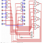
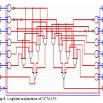
Using the Logisim, the basic components, D-type FF, IC 7474 (Dual D-FF), Multiplexer, IC 74153 (Dual 4×1 MUX) and Multiplexer, IC 74157 (Quad 2×1 MUX) have been developed as shown in Figures 3, 4 and 5 respectively.
Conclusion
In this paper, a novel Gray encoder/counter design has been presented. The novelty in the design returns to the unique combination of FF and MUXs along with the implemented triggering method. The presented design is based upon the D-type FF and MUX combination. The design underlying principle of operation stems from the creation of suitable BFs for each encoded bit waveform. This permitted a design that is modular for each stage of encoded bit. The modular solution of successive stages has also been advantageous to the design in two ways, returning to the fact that successive stage trigger rates are half that of their preceding stage counterparts. This unique triggering feature should allow both power consumption and heat dissipation to be lower compared to other designs with similar functionality. Besides both of these advantages, the design is flexible as it can switch between a counter or encoder mode as required. Furthermore, by incrementing the number of stages, the GC can either count over an extended time duration or count with a finer time resolution.
Acknowledgment
The authors would like to express their great appreciations and gratitude to Sultan Qaboos University, Sultanate of Oman for providing research facilities, technical supports and research environment.
References
- F. Gray, “Pulse code communication.” United States Patent Number 2,632,058, March 17, 1953.
- I. Flores, “Reflected number systems.” IRE Trans. Electronics & Computer.1956;5(2):79-82.
CrossRef
- F. G. Heath. “Origins of the binary code.” Scientific American.1972;227(2):76.
CrossRef
- A. Ahmad, and A. Al-Maashri. “Design and analysis of newly innovated set of binary code-words of unitary Hamming distance.” Proceedings IEEE international conference on communication, computer and power (ICCCP’07), Muscat, Oman.2007; Feb. 19 – 21:62 – 168
- T. N. Kwan, S. Chen, F. Boussaid and A. Bermak. “Compact Gray-code counter/memory circuits for spiking pixels.” Proceedings Fourth IEEE International Symposium on Electronic Design, Test and Applications – DELTA 2008, Hong Kong, SAR, China, 23-25.January 2008:506-511
- S.V. Yarmolik and V.N. Yarmolik. “Modified Gray and counter sequences for memory test address generation.” Proceedings of the International Conference, Mixed Design of Integrated Circuits and System.2006;(MIXDES 2006):.572-576
CrossRef
- H. Mehta, R. M. Owens and M. J. Irwin. “Some issues in Gray code addressing.” Proceedings of the 6th Great Lakes Symposium on VLSI.1196:178-181
CrossRef
- C. L. Su, C. Y. Tsui and A. Despain. “Saving power in the control path of embedded processors.” Proceedings of IEEE Design and Test of Computers.1994:24-31.
CrossRef
- C. L. Su, M. Alvin and A. Despain. “Cache design trade-offs for power and performance optimization: A Case Study. ISLPD.1995:63-68
CrossRef
- A. Maheshwari, W. Burleson and T. Russell. “Trading off reliability and power consumption in ultra-low power systems.” Proceedings International Symposium on Quality Electronic Design.2002:361–366.
CrossRef
- R. Hakenes and Y. A. Manoli. “Segmented gray code for low-power micro controller address buses.” Proceedings of 25th EUROMICRO Conference.1999;1:240 – 243.
CrossRef
- A. Ahmad, D. Ruelens, M. H. A. Awadalla and S. Ahmad. “An optimized technique for machine state reduction,” The Third International Conference on Numerical Analysis and Optimization NAOiii-2014, held at Sultan Qaboos University, Oman, January 5-9, 2014, Book Program & Abstracts, p. 36.
- S. Kundu, K. S. Krishna and S. Chattopadhyay. “Test pattern selection and customization targeting reduced dynamic and leakage power consumption.” Proceedings Asian Test Symposium., CD-ROM Proceedings. November 2009.
CrossRef
- S. Kundu and S. Chattopadhyay. “Scan-chain masking technique for low power circuit testing.” Proceeding of ASQED.2009:183-188
CrossRef
- M. V. Rao, N. S. Sravani and S. P. V. A. Brahmanandam. “Self-test techniques in SoC for low power consumption.” Int. J. Comp. Tech. Appl.2011;2(6):903-1906.
- N. Gupta. “Reduce SoC power use without high level EDA tools.” EE Times-Asia.2013:1-4
- A. Ahmad. “Another Perspective in Generation and using of Gray Code-words.” Journal of Electrical Engineering, IEEE Malaysia, (ELEKTRIKA).2007;9(2):49–55.
- A. Ahmad, and M. M. Bait Suwailam. “Design of an efficient and less memory requiring algorithmic procedure for computing Gray codes.” Proceedings IEEE international conference on communication, computer and power (.ICCCP’07), Muscat, Oman.2007; Feb. 19 – 21:172 – 176.
CrossRef
- A. Ahmad and M. M. Bait Suwailam. “A less complex algorithmic procedure for computing Gray codes.” The Journal of Engineering Research.2009;6(2):12-19.
CrossRef
- A. Ahmad and F. Bait-Shiginah. “A non conventional approach to generating efficient binary Gray code sequences.” IEEE Potentials.2012;31(3):16-19.
CrossRef
- Wikipedia—rotary encoder [Online]. Available at: http://en.wikipedia.org/wiki/Rotary_encoder
- C. Burch, C, “Logisim: A graphical system for logic circuit design and simulation.” Journal of Educational and Resources in Computing.2002;2(1)5-16.
CrossRef

This work is licensed under a Creative Commons Attribution 4.0 International License.
 and Medhat Awadalla